We are independent & ad-supported. We may earn a commission for purchases made through our links.

Advertiser Disclosure

Our website is an independent, advertising-supported platform. We provide our content free of charge to our readers, and to keep it that way, we rely on revenue generated through advertisements and affiliate partnerships. This means that when you click on certain links on our site and make a purchase, we may earn a commission. Learn more.

How We Make Money

We sustain our operations through affiliate commissions and advertising. If you click on an affiliate link and make a purchase, we may receive a commission from the merchant at no additional cost to you. We also display advertisements on our website, which help generate revenue to support our work and keep our content free for readers. Our editorial team operates independently from our advertising and affiliate partnerships to ensure that our content remains unbiased and focused on providing you with the best information and recommendations based on thorough research and honest evaluations. To remain transparent, we’ve provided a list of our current affiliate partners here.

What is Optical Lithography?

By Darlene Goodman
Updated May 17, 2024
Our promise to you
AboutMechanics is dedicated to creating trustworthy, high-quality content that always prioritizes transparency, integrity, and inclusivity above all else. Our ensure that our content creation and review process includes rigorous fact-checking, evidence-based, and continual updates to ensure accuracy and reliability.

Our Promise to you

Founded in 2002, our company has been a trusted resource for readers seeking informative and engaging content. Our dedication to quality remains unwavering—and will never change. We follow a strict editorial policy, ensuring that our content is authored by highly qualified professionals and edited by subject matter experts. This guarantees that everything we publish is objective, accurate, and trustworthy.

Over the years, we've refined our approach to cover a wide range of topics, providing readers with reliable and practical advice to enhance their knowledge and skills. That's why millions of readers turn to us each year. Join us in celebrating the joy of learning, guided by standards you can trust.

Editorial Standards

At AboutMechanics, we are committed to creating content that you can trust. Our editorial process is designed to ensure that every piece of content we publish is accurate, reliable, and informative.

Our team of experienced writers and editors follows a strict set of guidelines to ensure the highest quality content. We conduct thorough research, fact-check all information, and rely on credible sources to back up our claims. Our content is reviewed by subject matter experts to ensure accuracy and clarity.

We believe in transparency and maintain editorial independence from our advertisers. Our team does not receive direct compensation from advertisers, allowing us to create unbiased content that prioritizes your interests.

Optical lithography is a chemical process usually used in making computer chips. Flat wafers, often made from silicon, are etched with patterns to create integrated circuits. Typically, this process involves coating the wafers in chemical resist material. The resist is then removed to reveal the circuit pattern, and the surface is etched. The manner of removing the resist involves exposing the light-sensitive resist to visible or ultraviolet (UV) light, which is where the term optical lithography came from.

The main factor in optical lithography is light. Much like photography, this process involves exposing light-sensitive chemicals to beams of light in order to create a patterned surface. Unlike photography, though, lithography usually uses focused beams of visible — or more commonly, UV — light to create a pattern on a silicon wafer.
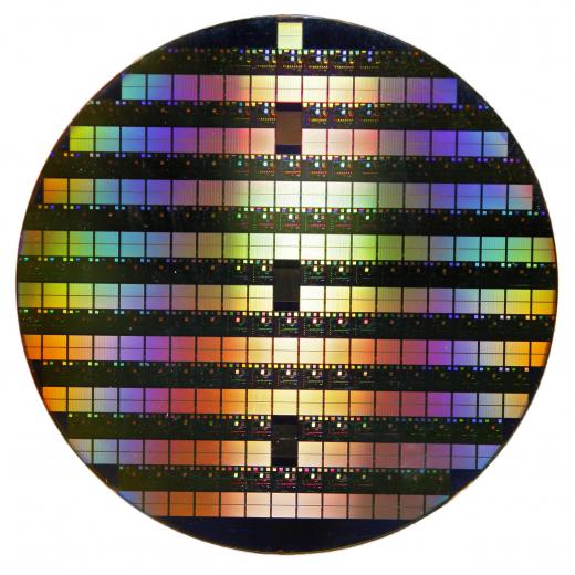
The first step in optical lithography is to coat the wafer’s surface in chemical resist material. This viscous liquid creates a light-sensitive film on the wafer. There are two types of resist, positive and negative. Positive resist dissolves in developer solution in all the areas where it is exposed to light, while negative ones dissolve in areas that were kept out of the light. Negative resist is more commonly used in this process, because it is less likely to distort in the developer solution than positive.

The second step in optical lithography is to expose the resist to light. The goal of the process is to create a pattern on the wafer, so the light is not emitted uniformly over the entire wafer. Photomasks, often made of glass, are typically used to block the light in areas that the developers do not want exposed. Lenses are also typically used to focus the light on particular areas of the mask.

There are three ways that the photomasks are used in optical lithography. First, they may be pressed against the wafer to block the light directly. This is called contact printing. Defects on the mask or the wafer may allow light onto the resist surface, thereby interfering with the pattern resolution.

Second, the masks may be held at close proximity to the wafer, but not touch it. This process, called proximity printing, reduces the interference from defects in the mask, and also allows the mask to avoid some of the extra wear and tear associated with contact printing. This technique can produce light diffraction between the mask and the wafer, which may also lessen the precision of the pattern.

The third, and most commonly used, technique for optical lithography, is called projection printing. This process sets the mask at a greater distance from the wafer, but uses lenses between the two to target the light and reduce diffusion. Projection printing typically creates the highest resolution pattern.

Optical lithography involves two final steps after the chemical resist is exposed to light. The wafers are typically washed with developer solution to remove positive or negative resist material. Then, the wafer is typically etched in all the areas where the resist no longer covers. In other words, the material 'resists' the etching. This leaves parts of the wafer etched and others smooth.

AboutMechanics is dedicated to providing accurate and trustworthy information. We carefully select reputable sources and employ a rigorous fact-checking process to maintain the highest standards. To learn more about our commitment to accuracy, read our editorial process.

Discussion Comments

AboutMechanics, in your inbox

Our latest articles, guides, and more, delivered daily.

AboutMechanics, in your inbox

Our latest articles, guides, and more, delivered daily.